LN 8: ICUP, I See You Process
Standard: CPU
Loading content...
Standard: CPU
In LN7, we developed a formal framework for parallel programming:
We now know when and why to parallelize. But all of that theory ultimately runs on physical hardware. Today we open the lid and look inside.
💡 Key Theme: As programmers, we constantly use abstraction layers to compartmentalize our work. But understanding the hardware beneath those abstractions gives us a much deeper appreciation for why our designs work the way they do — and how to make them better.
Before we build our own CPU from scratch, let's see what real ones look like. These are die shots — photographs of actual CPU silicon taken under a microscope after the metal heat spreader is removed.
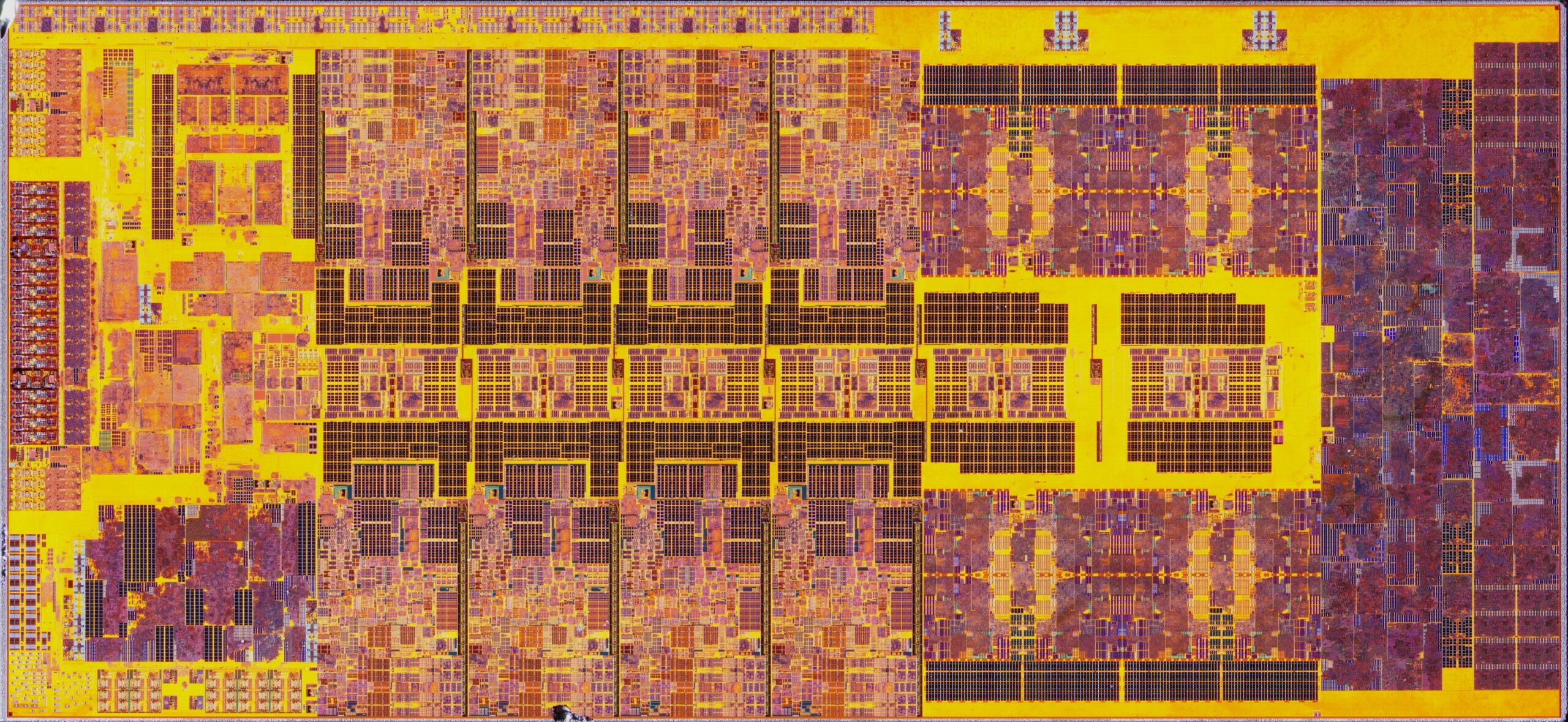
Intel 12900K (Alder Lake, 2021) — ~billion transistors, 10nm
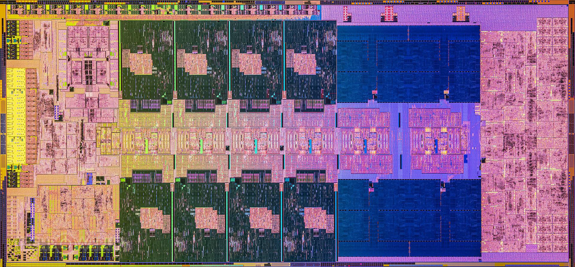
Intel 13900K (Raptor Lake, 2022) — Intel 7 process
Notice a few things in the labeled views:
📚 Moore's Law: The Intel 4004 (1971) — the first commercial microprocessor — had 2,300 transistors. The 12900K has roughly billions. That's a factor of ~10 million in 50 years. Each generation of improvements to the components we're about to study made this possible.
Now let's build our own understanding from the ground up. Here's our empty CPU shell — we'll fill it in piece by piece as we learn each component:
Our CPU — Empty Shell
Before putting anything inside our CPU, we need to decide what language it speaks. The Instruction Set Architecture defines the interface between software and hardware — the set of instructions the processor understands.
The two dominant philosophies for designing an ISA are CISC and RISC — and they represent fundamentally different bets on where to put complexity.
Examples: x86 (Intel/AMD), VAX, Motorola 68000
CISC processors have a vast vocabulary of specialized instructions. Some instructions are so powerful they can read from memory, perform arithmetic, and write the result back — all in a single instruction.
| Characteristic | CISC |
|---|---|
| Instruction count | Hundreds to thousands |
| Instruction length | Variable (1-15 bytes on x86) |
| Memory access | Some instructions access memory directly |
| Optimization goal | Reduce memory accesses via powerful instructions |
| Complexity | In the hardware (microcode) |
; x86 CISC: one instruction does memory read + add + memory write
ADD [memory_address], 42
🤔 The thinking: In the 1970s-80s, memory was extremely slow and expensive. Compilers were primitive. Putting more power into each instruction meant fewer total instructions, which meant fewer slow memory fetches for the program itself.
Examples: ARM, MIPS, RISC-V, SPARC, PowerPC
RISC processors use a small, simple set of foundational instructions. Each instruction does one thing well. Only dedicated load and store instructions touch memory — everything else operates on registers.
| Characteristic | RISC |
|---|---|
| Instruction count | Dozens to low hundreds |
| Instruction length | Fixed (4 bytes on ARM/RISC-V) |
| Memory access | Only via load/store instructions |
| Optimization goal | Throughput via pipelining |
| Complexity | In the compiler |
; ARM RISC: three instructions for the same operation
LDR R1, [memory_address]   ; Load from memory into register
ADD R1, R1, #42            ; Add 42 to register
STR R1, [memory_address]   ; Store register back to memory
🤔 The thinking: Simple, uniform instructions can flow through a pipeline like an assembly line. While one instruction is being executed, the next is being decoded, and the one after that is being fetched — all simultaneously. Fixed-length instructions make this pipeline clean and predictable.
In the early 1980s, David Patterson (Berkeley) and John Hennessy (Stanford) made a revolutionary observation: measurements of real programs showed that 80% of execution time was spent on just 20% of the instruction set. All those complex CISC instructions? Rarely used. Their research led to the RISC architecture — and Patterson and Hennessy won the Turing Award in 2017 for this work.
Here's the twist: modern x86 processors are actually RISC inside. Starting with Intel's Pentium Pro (1995), x86 chips decode complex CISC instructions into simple RISC-like micro-operations (μops) internally. The outside speaks CISC (for backwards compatibility), but the inside executes RISC (for pipeline efficiency). The best of both worlds!
📌 Key Insight: The die shots we looked at earlier? Those P-cores are running a RISC micro-engine underneath the CISC instruction decoder. The ISA is a contract, but the implementation can be anything.
Two other architectural designs are worth knowing:
Examples: Intel IA-64 (Itanium), DSP chips, some GPUs
VLIW bundles multiple operations into one very long instruction. The compiler decides which operations can execute in parallel and packs them together. The hardware just executes what it's told — no dynamic scheduling.
; VLIW: compiler bundles 3 operations into one instruction
{ ADD R1, R2, R3 | MUL R4, R5, R6 | LOAD R7, [addr] }
💀 Historical Disaster — The Itanium: Intel bet billions on IA-64/Itanium, a VLIW architecture called EPIC (Explicitly Parallel Instruction Computing). The bet was that compilers could schedule parallelism better than hardware. They couldn't — the problem turned out to be too hard for static analysis. Meanwhile, x86 processors got better at dynamic scheduling, and ARM won the efficiency war. Itanium was discontinued in 2021 after two decades of poor adoption. It's one of the most expensive failed bets in computing history.
Examples: Intel SSE/AVX, ARM NEON, WebAssembly SIMD
SIMD extends the ISA with vector registers that hold multiple data elements. One instruction operates on all elements simultaneously.
; SIMD: one instruction adds 4 pairs of numbers at once
VADDPS ymm0, ymm1, ymm2   ; Add 8 floats in parallel!
This is enormously powerful for image processing, scientific computing, machine learning, and games.
Rust SIMD example — reaching down to the ISA level:
#[cfg(target_arch = "x86_64")]
use std::arch::x86_64::*;

unsafe fn simd_add(a: &[f32; 4], b: &[f32; 4]) -> [f32; 4] {
    let va = _mm_loadu_ps(a.as_ptr());  // Load 4 floats into vector register
    let vb = _mm_loadu_ps(b.as_ptr());  // Load 4 more floats
    let vc = _mm_add_ps(va, vb);        // Add all 4 pairs simultaneously!
    let mut result = [0.0f32; 4];
    _mm_storeu_ps(result.as_mut_ptr(), vc);
    result
}
💡 Connection to LN7: See how these ISA designs map directly to our parallelism strategies?
ISA Design Parallelism Strategy LN7 Analogy RISC + Pipeline Task parallelism Car wash — instructions flow through stages SIMD Data parallelism Machine shop — same operation on many data items VLIW Task parallelism (static) Compiler-scheduled pipeline Superscalar CISC Both Modern x86 does both internally
One more ISA-level choice that trips up every systems programmer eventually: byte ordering.
| Endianness | Byte Order | Used By |
|---|---|---|
| Little-endian | Least significant byte first | x86, ARM (default), RISC-V |
| Big-endian | Most significant byte first | Network protocols, some MIPS, older SPARC |
The number 0x12345678 stored at address 0:
Little-endian: [78] [56] [34] [12]   (address 0 → 3)
Big-endian:    [12] [34] [56] [78]   (address 0 → 3)
⚠️ Gotcha: Network byte order is big-endian, but x86 is little-endian. Every network program must convert. Rust's
u32::to_be_bytes()andu32::from_be_bytes()exist specifically for this.
Now let's add the first component to our CPU. Registers are the fastest storage in the entire computer — they sit inside the CPU itself, accessed in a fraction of a nanosecond.
Registers Added
GPRs are the CPU's scratch paper — the working memory for all computations.
| Architecture | GPR Count | Names | Register Size |
|---|---|---|---|
| x86-64 | 16 | RAX, RBX, RCX, RDX, RSI, RDI, RBP, RSP, R8-R15 | 64-bit |
| ARM (AArch64) | 31 | X0-X30 | 64-bit |
| RISC-V (RV64) | 32 | x0-x31 | 64-bit |
More GPRs = less pressure to spill values to memory. ARM's 31 registers vs x86's 16 means ARM code needs fewer memory accesses on average — a direct advantage of the clean RISC design.
💡 Connection to Rust: When you declare
let x = 42;, the compiler tries to keepxin a register. This is called register allocation — one of the most important compiler optimizations. If there aren't enough registers, the compiler "spills" the variable to the stack (memory), which is orders of magnitude slower.
These registers have dedicated hardware roles that keep the CPU running:
| Register | Full Name | Purpose |
|---|---|---|
| IP/PC | Instruction Pointer / Program Counter | Address of the next instruction to fetch |
| IR | Instruction Register | Holds the instruction currently being executed |
| SP | Stack Pointer | Points to the top of the stack |
| BP/FP | Base Pointer / Frame Pointer | Points to the base of the current stack frame |
| ACC | Accumulator | Stores the result of ALU operations |
| FLAGS | Flag/Status Register | Condition codes: zero, carry, overflow, sign, etc. |
| MAR | Memory Address Register | Holds the address to read from or write to in RAM |
| MBR/MDR | Memory Buffer/Data Register | Holds data going to or coming from RAM |
📌 How they work together: In the simplified fetch/decode/execute model, when the CPU executes
ADD RAX, 5:
- PC tells the CPU where to find this instruction in memory
- MAR receives the address from PC, sends it to the memory bus
- MBR receives the instruction bytes from memory
- IR stores the decoded instruction: "ADD the value 5 to RAX"
- The ALU performs the addition, result goes to ACC then RAX
- FLAGS is updated (was the result zero? did it overflow?)
- PC is incremented to the next instruction
As an important note, these are a generalized look at many special registers, they are NOT always present in all architectures!
x86 register names carry the scars of five decades of backwards compatibility:
1974 (8080):     A          (8-bit accumulator)
1978 (8086):     AX         (16-bit: AH + AL)
1985 (80386):    EAX        (32-bit: Extended AX)
2003 (AMD64):    RAX        (64-bit: Register AX)
Every generation extended the previous register rather than starting fresh. That's why x86 register names are inconsistent (RAX, RBX, RCX... then R8, R9, R10) while ARM has clean X0-X30 — ARM had the luxury of starting from scratch.
📚 Historical Note — SPARC Register Windows: Sun's SPARC architecture (1987) tried a different approach: instead of saving and restoring registers on function calls, the hardware rotated a window over a large register file of 128+ registers. Each function got a fresh "view" of registers without any memory operations. Clever, but the large register file was expensive, and the approach fell out of favor.
The ALU is literally the base of operations — the hardware where computation physically happens. Every addition, comparison, and logical operation your program performs ultimately executes here.
ALU Added
| Category | Operations | Flag Effects |
|---|---|---|
| Arithmetic | ADD, SUB, MUL, DIV, increment, decrement | Sets carry, overflow, zero, sign |
| Logical | AND, OR, XOR, NOT, bit shifts, rotates | Sets zero, sign |
| Comparison | CMP (subtract without storing), TEST (AND without storing) | Sets all condition flags |
The result is written to the destination register chosen by the instruction, and the FLAGS register is updated to reflect the outcome. This is how if statements work at the hardware level — the compiler emits a CMP instruction, then a conditional jump that checks the flags.
A pipelined ALU breaks each operation into stages that execute in sequence. While one instruction is in the "execute" stage, another is in "decode," and a third is being "fetched":
Time →    t0    t1    t2    t3    t4
Stage 1:  I1    I2    I3    I4    I5     ← Fetch
Stage 2:  ---   I1    I2    I3    I4     ← Decode
Stage 3:  ---   ---   I1    I2    I3     ← Execute

Result: After initial fill-up, one instruction completes every cycle!
💡 Connection to LN7: This is task parallelism at the hardware level — exactly the car wash analogy! Each pipeline stage is a "station" doing one specialized job. Instructions are "cars" flowing through.
A superscalar CPU has multiple ALUs operating in parallel. If two instructions are independent, they can execute simultaneously:
Time →    t0    t1    t2
ALU 1:    I1    I3    I5
ALU 2:    I2    I4    I6

Result: Two instructions complete every cycle!
💡 Connection to LN7: This is data parallelism — the machine shop analogy! Multiple "mechanics" (ALUs) working on different "cars" (instructions) simultaneously.
A notorious example of what happens when ALU hardware has a defect. Intel's Pentium processor had a bug in its floating-point division lookup table — certain specific inputs produced incorrect results.
Correct:  4195835.0 / 3145727.0 = 1.333820449136241002
Pentium:  4195835.0 / 3145727.0 = 1.333739068902037589
                                          ^^^ Wrong!
Intel initially dismissed the issue, claiming it would only affect one in nine billion random divisions. But the math and science community was outraged — you can't have a CPU that sometimes gives wrong answers. Intel was forced to offer a full recall, costing approximately $475 million.
⚠️ Lesson: You can't "patch" a logic gate. Hardware verification is absolutely critical — a bug in the ALU affects every program that runs on it. This is why formal verification of CPU designs is a major field of research.
Briefly note: hardware multiplication requires far more transistors and clock cycles than addition. A 64-bit multiplier circuit is roughly 10x more complex than an adder. This is why:
x << 1 instead of x * 2) was historically a real optimizationThe Control Unit is the conductor of the orchestra. It doesn't perform computation itself — it tells every other component what to do and when to do it. It maintains communication among all CPU hardware and manages the fetch-decode-execute cycle.
Control Unit Added
Every instruction your program runs goes through this fundamental cycle:
    ┌─────────────────────────────────────────────┐
    │                                             │
    ▼                                             │
┌─────────┐    ┌──────────┐    ┌───────────┐     │
│  FETCH   │───▶│  DECODE  │───▶│  EXECUTE  │─────┘
│          │    │          │    │           │
│ Read PC  │    │ Read IR  │    │ Generate  │
│ Load IR  │    │ Parse:   │    │ control   │
│ Update   │    │ - opcode │    │ signals   │
│ PC       │    │ - operands│   │ Move data │
│          │    │ - mode   │    │ Write     │
│          │    │          │    │ results   │
└─────────┘    └──────────┘    └───────────┘
1. Fetch:
2. Decode:
3. Execute:
This cycle repeats billions of times per second on a modern CPU.
The CU is also the security gatekeeper. Based on the current privilege level (which we'll cover next), it can enable or disable certain instructions. A user-mode program trying to execute a privileged instruction? The CU generates an exception instead of executing it.
| Design | Mechanism | Speed | Updateable? | Used In |
|---|---|---|---|---|
| Hardwired | Fixed logic circuits (combinational logic) | Fast | No — burned into silicon | Embedded, RISC |
| Microprogrammed | Microcode instructions in flashable ROM | Slower | Yes — firmware updates! | CISC, x86 |
Hardwired CUs use pure combinational logic gates — the decoding is literally wired into the chip. They're fast, cheap, and simple, but can never be changed after manufacturing. Perfect for simple RISC processors and embedded systems where the ISA is small and stable.
Microprogrammed CUs store a small program (microcode) in ROM that translates each ISA instruction into a sequence of micro-operations. The microcode can be updated via firmware patches — which turned out to be extraordinarily important in 2018.
Modern CPUs include a major optimization called speculative execution. When the CPU hits a branch (if/else), it may predict which path is likely and begin work early. If the guess is right, it saves time. If not, the architectural results are rolled back.
In January 2018, researchers discovered that this optimization created catastrophic security vulnerabilities:
These vulnerabilities affected a huge range of modern CPUs. Spectre was broadly cross-vendor; classic Meltdown was especially associated with Intel and some ARM designs. Software patches reduced performance by 5-30% on some workloads.
💡 Key Connection: The Spectre/Meltdown mitigations were partly delivered as microcode updates — patches to the microprogrammed CU. This is exactly why microprogrammed CUs exist! A hardwired CU would have required a physical chip replacement. The flexibility to update microcode literally saved the industry from having to recall billions of processors.
Now we add the security hardware that protects the CPU from misuse. All of this complex machinery we've built needs safeguards — otherwise any program could execute any instruction, including ones that corrupt the OS or other programs.
Security Ring Added
Most modern operating systems use just two privilege levels:
| Ring | Name | Access | Who Runs Here |
|---|---|---|---|
| Ring 0 | Kernel Mode | Full, unrestricted access to all hardware | OS kernel, device drivers |
| Ring 3 | User Mode | Restricted — privileged instructions are disabled | Applications, user programs |
How it works: A hardware bit in the CPU Mode Register stores the current privilege level. When this bit indicates Ring 3 (user mode), the Control Unit physically prevents execution of privileged instructions like:
Instead, user programs must use the system call interface — a controlled gateway that transitions to Ring 0, lets trusted kernel code perform the operation, and returns to Ring 3.
The x86 hardware actually defines four rings (Ring 0 through Ring 3). The original vision:
| Ring | Intended Use |
|---|---|
| Ring 0 | OS Kernel |
| Ring 1 | Device Drivers |
| Ring 2 | Privileged Services |
| Ring 3 | User Applications |
But Linux and Unix systems only ever used Ring 0 and Ring 3. As these systems became dominant, software was only designed for the two-ring model. Windows followed suit — even though the x86 hardware supports four rings, virtually all modern operating systems only use two. Rings 1 and 2 are vestigial hardware features, mostly unused.
Modern processors have privilege levels that go below Ring 0:
Ring -1 — Hypervisor Mode (Intel VT-x / AMD-V): A privilege level beneath the kernel, designed for virtual machine monitors (hypervisors). The hypervisor controls which "Ring 0" kernel code each virtual machine gets to run. This is what makes cloud computing possible — services like AWS run your OS in a VM, with the hypervisor ensuring VMs can't interfere with each other.
Ring -2 — System Management Mode (SMM): Triggered by special hardware events like overheating, power management, or firmware operations. The BIOS/UEFI firmware handles these events in a mode that is invisible to the operating system itself. When SMM activates, the CPU pauses everything (including the OS), handles the event, and resumes — the OS never knows it happened.
This security model is enforced by a collection of dedicated hardware:
| Hardware | Role |
|---|---|
| CPU Mode Register | Stores the current privilege level as bits |
| Interrupt/Exception Handler | Triggers mode switches on page faults, syscalls, invalid opcodes |
| MMU (Memory Management Unit) | Prevents unauthorized memory access via page table permissions |
| System Call Interface | The controlled gateway between User and Kernel mode |
MMU Added
The MMU deserves special mention: it translates virtual addresses (what your program sees) to physical addresses (where data actually lives in RAM). Each page of memory has permission bits — read, write, execute, and which ring can access it. A user-mode program trying to access kernel memory? The MMU triggers a page fault exception, which the interrupt handler routes to the OS for handling (usually: kill the offending process).
The first major internet worm exploited a buffer overflow — a failure to enforce memory boundaries. A program on a networked Unix machine received more data than its buffer could hold, overwriting the return address on the stack and redirecting execution to attacker-controlled code. The worm infected approximately 10% of the internet (about 6,000 machines — the internet was small then).
This incident led to the creation of CERT (Computer Emergency Response Team) and drove decades of investment in hardware memory protection. The MMU, privilege rings, and stack protections we have today are the direct legacy of attacks like this.
The final piece of our CPU. Everything we've built so far runs in isolation — the fetch-decode-execute cycle would just loop through instructions forever. But real computers need to respond to the outside world: keyboard presses, mouse clicks, network packets, timers. That's what interrupts are for.
Complete CPU!
When a device needs the CPU's attention:
1. Device sends signal (e.g., keyboard key pressed)
   │
   ▼
2. Interrupt Controller routes the signal to the CPU
   │
   ▼
3. CPU finishes current instruction
   │
   ▼
4. CPU saves its state (registers, PC, FLAGS → stack)
   │
   ▼
5. CPU looks up the ISR address in the Interrupt Vector Table
   │
   ▼
6. CPU jumps to the ISR (Interrupt Service Routine)
   │
   ▼
7. ISR handles the event (read keycode, update buffer, etc.)
   │
   ▼
8. ISR signals completion
   │
   ▼
9. CPU restores saved state (stack → registers, PC, FLAGS)
   │
   ▼
10. CPU resumes previous execution exactly where it left off
| Type | Source | Example | Trigger |
|---|---|---|---|
| Hardware (External) | Physical devices | Keyboard press, mouse click, network packet, timer tick | Signal on interrupt pin |
| Software (Trap) | Programs | System call (int 0x80), breakpoint (int 3) | Special instruction |
| Exception | CPU itself | Division by zero, page fault, invalid opcode | Error during execution |
Here's a fun application of interrupt knowledge. When your computer "freezes" — maybe a program is stuck in an infinite loop hogging the CPU — you may still notice that the mouse cursor moves on screen.
Why? Because mouse input is a hardware interrupt. Even when a program has the CPU locked in a tight loop, the interrupt controller can still signal the CPU. The CPU briefly pauses the stuck program, handles the mouse ISR (update cursor position, redraw), and returns. The stuck program never knows it was interrupted.
Now here's the diagnostic insight: if the mouse cursor also freezes, it means the CPU isn't even handling certain hardware interrupts anymore! This indicates a much more serious problem — the CPU might be stuck in an ISR itself, or interrupts have been disabled. A hard crash is likely imminent. The diagnostic escalation:
| Symptom | What It Means | Severity |
|---|---|---|
| Program unresponsive, mouse moves | Program is stuck, but CPU handles interrupts | Moderate — kill the process |
| Mouse cursor frozen | CPU not processing interrupts | Severe — system may recover |
| Screen frozen, no response | CPU completely halted or in error loop | Critical — hard reboot needed |
💡 Another fun one — Ctrl+C: When you press Ctrl+C in a terminal, the terminal sends a SIGINT signal — which is delivered via an interrupt. The OS's signal handler terminates the running process. If Ctrl+C doesn't work, it means the process has either masked that signal or the system is too unresponsive to process interrupts.
Not all interrupts are created equal. A disk I/O completion shouldn't preempt a power-failure handler. CPUs implement interrupt priority levels — higher-priority interrupts can preempt lower-priority ISRs:
| Priority | Example | Can Be Masked? |
|---|---|---|
| Highest | NMI (Non-Maskable Interrupt) — hardware failure | No — always handled |
| High | Timer tick — scheduling quantum expired | Depends on context |
| Medium | Disk I/O completion | Yes |
| Low | Keyboard input | Yes |
Masking means temporarily disabling certain interrupts. The OS does this during critical sections — for example, while updating the interrupt table itself. But NMI (Non-Maskable Interrupt) can never be masked — it's reserved for critical events like hardware failure and memory parity errors where the CPU must respond immediately.
Let's take one final look at our fully assembled CPU. Every component we've learned works together:
Complete CPU Architecture
The Control Unit orchestrates the fetch-decode-execute cycle, reading instructions and generating signals. The Registers provide ultra-fast scratch storage. The ALU performs the actual computation. The Ring/Mode Register enforces privilege levels. The MMU protects memory. The Interrupt Handler connects the CPU to the outside world.
This is the bedrock on which our compilers generate instructions. Every programming language — Rust, Python, Java — is ultimately a high-level abstraction of the decisions made here. This is where logic meets metal.
📌 Callback to the die shots: Now look at those labeled die photos again. Can you identify the regions that correspond to the components we've studied? The register files, the execution units (ALUs), the control logic, the memory interface — they're all visible in silicon.
We've built a complete single-core CPU model. But modern processors are far more complex. Here's a preview of what lies beyond:
The die shots showed multiple cores — each one is essentially a complete copy of everything we've studied (registers, ALU, CU, etc.), all on one chip. Cores share some resources (L3 cache, memory controller) but have their own private resources (L1/L2 cache, register file). This is why threads on different cores can execute truly in parallel — they have separate hardware.
As we discussed in LN7's "Know Your Hardware" section, caches dominate the die area. The hierarchy (L1 → L2 → L3 → RAM) bridges the enormous speed gap between registers (~0.3ns) and main memory (~100ns). Cache design involves deep tradeoffs in associativity, replacement policies, and coherence protocols that keep multiple cores' caches consistent.
The MMU we mentioned contains the TLB (Translation Lookaside Buffer) — a cache of recent virtual-to-physical address translations. Page tables, page walks, and TLB misses are critical performance factors we'll explore in LN14-16 on memory management.
Modern systems use an APIC (Advanced Programmable Interrupt Controller) that can route interrupts to specific cores, coalesce multiple interrupts, and support MSI (Message Signaled Interrupts) where devices write directly to memory instead of using dedicated interrupt pins.
| Component | Role | Key Insight |
|---|---|---|
| ISA | Contract between software and hardware | CISC vs RISC: complexity in hardware vs compiler |
| Registers | Ultra-fast CPU storage (~0.3ns) | GPRs for data, SPRs for control (PC, SP, FLAGS) |
| ALU | Where computation physically happens | Pipelined (task parallel) or superscalar (data parallel) |
| Control Unit | Orchestrates fetch-decode-execute | Hardwired (fast, fixed) vs microprogrammed (updateable) |
| Privilege Rings | Hardware security enforcement | Ring 0 (kernel) vs Ring 3 (user), plus hypervisor/SMM |
| MMU | Memory protection and translation | Virtual → physical addresses, page-level permissions |
| Interrupts | External world communication | Save state → handle ISR → restore state → resume |
Key Definitions:
| Term | Definition |
|---|---|
| ISA | Instruction Set Architecture — the contract between software and hardware |
| CISC | Complex Instruction Set Computing — many powerful, variable-length instructions |
| RISC | Reduced Instruction Set Computing — few simple, fixed-length instructions |
| SIMD | Single Instruction, Multiple Data — vector operations on parallel data |
| ALU | Arithmetic Logic Unit — performs arithmetic, logic, and comparison operations |
| Control Unit | Orchestrates CPU operations via fetch-decode-execute cycle |
| Program Counter | Register holding the address of the next instruction |
| Privilege Ring | Hardware-enforced security level (Ring 0 = kernel, Ring 3 = user) |
| MMU | Memory Management Unit — translates virtual addresses, enforces permissions |
| Interrupt | Signal causing CPU to save state and jump to a handler routine |
| ISR | Interrupt Service Routine — the handler code for an interrupt |
| NMI | Non-Maskable Interrupt — cannot be disabled, reserved for critical events |
The Fetch-Decode-Execute Cycle:
FETCH  →  Read PC, load instruction into IR, increment PC
DECODE →  Parse opcode, operands, addressing mode from IR
EXECUTE → Generate control signals, perform operation, write results
ISA Comparison:
| Property | CISC | RISC |
|---|---|---|
| Instructions | Many, complex | Few, simple |
| Length | Variable | Fixed |
| Memory access | Some instructions access directly | Only load/store |
| Optimization | Reduce memory accesses | Pipeline throughput |
| CU design | Microprogrammed | Hardwired |